How To Order Solder Stencils And Save Big – Manufacturing, Material, And Information-Sharing
Developing new PCB-based solutions is always time-consuming, laborious, and expensive. That’s why in both hobbyist electronics projects and large-scale manufacturing processes, reducing the time and costs associated with the project is a key priority. That’s why soldering with stencils is so popular.
Stencils were designed to make solder pasting processes time and cost-efficient. In through-hole components, whipping out that iron to solder is easy, but working with SMD components is far more difficult. Dealing with super-small contact pad connections can make anyone’s hands clumsy hands.
Fortunately, with solder paste stencils, we receive benefits like –
- Each contact pad receives the same amount of solder paste.
- The assembled boards are more reliable.
- Instead of one pad at a time, soldering pros can apply solder paste to the entire board at once.
The more reliable the assembled boards, the lesser risk of waste generation. Every year, manufacturers across the world produce 45 million tons of waste electrical and electronic equipment (WEEE). At the core part of all this WEEE are waste printed circuit boards (WPCBs). Using stencils is also key to reducing the amount of solder paste and various other electronic components we waste.
So, how to order high-quality solder stencils that provide the best results? Our top three considerations are – manufacturing, material, and information-sharing. Let’s explore the three –
Manufacturing
To ensure solder joint reliability during surface mount assembly processes while dealing with the ever-shrinking sizes of electronic components, the top solder paste stencil manufacturers have developed state-of-the-art manufacturing techniques. Some of them include –
- Chemical Etching
- Laser Cutting
- Electroforming
Laser cutting, with the use of advanced YAG lasers, heavy-duty cutting tables, and precision servo motors, is the most efficient manufacturing technique. The manufacturing technique determines the quality of finishes on the surfaces of the stencil aperture walls.
The smoother these finishes, the easier it’ll be for the solder paste to be released from the stencils. That’s why customers are recommended to partner with solder paste stencil manufacturers that use laser-cutting techniques. Such manufacturers typically have process and design engineers on their teams.
These professionals review CAD data and modify the solder paste stencils’ apertures using industry-standard designs based on the IPC 7525 guidelines. The top manufacturers also offer customization options. They ask their clients to upload Gerber files and send check-plots for approval before starting the manufacturing process.
These are the characteristics stencil shoppers should look for in solder paste stencil manufacturers!
Materials
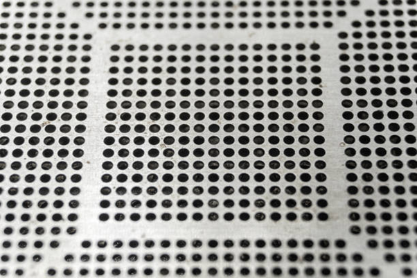
The molecular structure of Nickel and stainless-steel mixtures is ideal for laser-cutting. Stainless steel with high amounts of Nickel content provides the most accurate apertures (effective area ratios) in stencil manufacturing processes. Using this material, manufacturers create smooth aperture walls which enable precise releases of solder paste.
Precise releases of solder paste are extremely important in modern-day assembly processes. That’s because –
- Solder paste contains alloys and flux. In regions of the board where solder is applied, they assist in the reflow process.
- Insufficient release of solder paste means insufficient flux.
- Thus, the solder fails to hold components properly to the circuit board.
That’s why maintaining correct ratios of flux in the solder is extremely important. But, due to the demand for smaller components, very small amounts of solder paste are required in most assembly processes. Hence, solder stencils need to have super-small apertures as well.
When manufacturers decrease the circumferences of the apertures, they have no choice but to increase the thickness of the stencils. It’s the only way the stencils can hold the required amounts of paste. With thicker stencils, releasing the paste precisely is more difficult. There are also changes in the rates at which the solder paste is applied onto the stencils.
Thankfully, stencils made of Nickel and stainless-steel mixtures offer high degrees of dimensional stability. They can be used in non-stop printing procedures, irrespective of how fine-pitched the boards’ components are. Correct amounts of solder paste are always applied with these stencils.
That’s why customers are recommended to shop for stencils made of Nickel and stainless-steel mixtures.
Information Sharing
Now that we know what stencil material is the best and how to select the best stencil manufacturers, are you ready to order solder stencils? Your stencil seller may ask you to upload a set of Gerber files for your top/bottom paste layers. To generate Gerber files for your paste layers in EAGLE, you’ll need to –
- Open the PCB layout file on Autodesk EAGLE.
- Locate the “CAM Processor” icon; click on it.
- Unselect all default layers in the Cam Processor window.
- Select Layer 31 t-Cream.
- Go to the Output field.
- In the Device dropdown section, select Gerber_RS274X.
- In the File field section, give the stencil file a name.
- Click the “Process Job” option.
Your Gerber file will be generated! Find it in the project folder and upload it on the stencil seller’s website. If you’re still a bit confused about what stencil you need to choose, contact a reliable circuit board manufacturer for more information!